|
Silicon Burns !Carl Frosch and the Discovery of Oxidized Silicona remembrance by Mason ClarkA key process in the building of silicon devices is the step of burning an oxide layer onto the silicon wafer. The layer is the start of the photographic processes that create patterns on the surface. These patterns make up the devices and the interconnections of the integrated circuit. The oxide layer is a mask for localizing diffusion and metal deposition. In the words of Andy Grove in his 1967 book, "an exceedingly important factor in the development of planar technology." It was the over-throwing of a silicon dogma: "silicon burns". I'll tell its story from my own observation at the Bell Telephone Laboratory. I was developing germanium power transistors using a process called "alloying." It was difficult by alloying to produce flawless, flat p-n junction surfaces over large areas. A foreign particle or stain on the surface would cause a defect. An alternative was needed. It was also time to switch from germanium to silicon. Alloying p-n junctions on silicon would have this large-area defect problem -- especially troublesome in power transistors. An alternative to alloying might be the diffusion of dopants, the impurities to create "n" or "p" type layers. The first report of the alloying method was mistaken by some at the Schenectady General Electric laboratory to be diffusion, so the notion of diffused junctions, but not the reality, was introduced by this error. Research on diffusion was being done by Ditzenberger. To perform diffusion into silicon it was necessary to heat the silicon in a protective atmosphere, preferably vacuum or hydrogen, to avoid simply burning up the silicon. Carbon (you might say "coal") and silicon are first cousins in the periodic table. Each will surely burn if heated in air. So Ditzenberger and his assistant, Fuller, carefully sealed wafers of silicon in a quartz capsule together with the dopant and vacuum or hydrogen. By this means they provided data on the diffusion of boron and phosphorus into silicon and opened the path to large-area p-n junction perfection. But the technique was awkward to perform. Carl Frosch sought an alternative by heating the silicon in an open quartz tube, using a flow of hydrogen to prevent the silicon from burning. When I went looking for diffusion techniques for power transistors I found Carl in the fourth-floor attic of the Murray Hill laboratory. He didn't have a proper lab for his furnaces and bottles of hydrogen. His furnaces were the laboratory furnaces available in 1956, using two rods of silicon carbide as heating elements. In his make-shift laboratory he used hydrogen tanks and rubber tubing. He was just beginning to do diffusion by adding impurities to the hydrogen stream. The technique had promise of being more manufacturing-suitable than Ditzenberger's sealed quartz. The next time I visited Carl he had moved to a proper laboratory, a move that had historic importance. He was excited to show me his discovery. His silicon wafers had turned purple--a beautiful, uniform purple. What had happened? He and his assistant had hastened to inspect their system and correct the problem. Carl told us of the inspiration he had while he was driving home the evening of their purple disaster. He remembered that when they re-installed their furnace after the move there had been a problem with leaky rubber tubing in the hydrogen line. Air, i.e. oxygen, must have gotten into the furnace. So the next day they heated a silicon wafer without the flow of hydrogen -- in air. And there was the oxide layer on which the integrated-circuit industry rests. Highly pure, single-crystal, silicon forms a protective layer of oxide. Frosch quickly learned to selectively remove the oxide, using hydrofluoric acid, and reported, "Surface Protection and Selective Masking During Diffusion in Silicon," J. Electrochem. Soc., 104, 547 (1957) It was the accident of leaky tubing and the alertness of Carl Frosch that overcame the dogma that "silicon burns." K. D. Smith was puzzled by Carl's discovery and took out of his ample desk drawers a sample of the silicon used to make microwave diodes in World War II. This he placed in a furnace, in air, and confirmed that "silicon burns." The sample survived but looked like a particle of moss -- overgrown with dendrites of silicon and oxide. It was this early experience with polycrystalline silicon, along with the science of the periodic table, that had established in our minds that silicon must not be heated in oxygen. When I moved to Pacific Semiconductors a year later, a very competent doctor of chemistry warned me that I must not attempt to heat silicon in an open-tube furnace lest it simply burn up. "Look at the periodic table," he scolded. Fortunately, Carl Frosch had just published his paper proving otherwise. 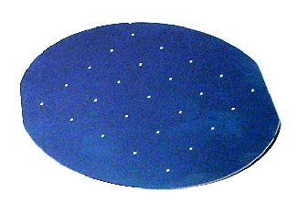 An oxidized silicon wafer with aluminum dots for evaluating the purity of the oxide layer. The oxide is colorless. The color seen is caused by interference between the reflections from the silicon and from the outer oxide surface. The color is used to measure the thickness of the oxide, which is about the wavelength of light.
Mason Clark was a member of the technical staff of the Bell Telephone Laboratories 1952 to 1957. He was supervisor of power transistor and microwave diode development. He became product development manager at Pacific Semiconductors (PSI) and later at Hewlett-Packard Associates. His web site covering his retirement interests is at
|
|
|